
Laboratoire Léon Brillouin
UMR12 CEA-CNRS, Bât. 563 CEA Saclay
91191 Gif sur Yvette Cedex, France
+33-169085241 llb-sec@cea.fr
Laboratoire Léon Brillouin
UMR12 CEA-CNRS, Bât. 563 CEA Saclay
91191 Gif sur Yvette Cedex, France
+33-169085241 llb-sec@cea.fr

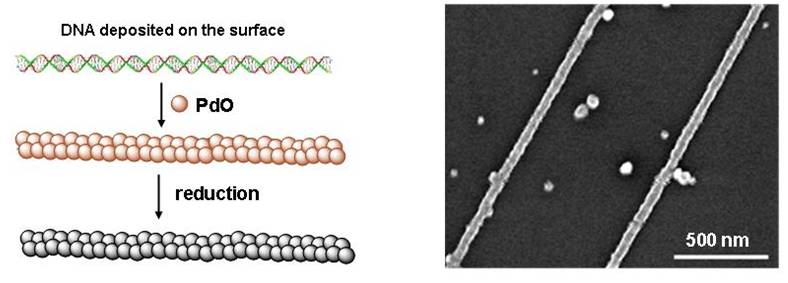
Scheme of the synthesis of palladium nanowires (left) and scanning electron microscopy image of palladium nanowires (right).
Thanks to the amazing selfassembly properties of DNA, structures of exquisite complexity can be built just in designing proper DNA sequences (DNA origami is the best example). They can be used in the further design of complex systems involving other nanoobjects, or for the preparation of functional devices. Our aim is to demonstrate the fabrication of carbon nanotube transistors by selfassembly on a DNA structure. DNA is used here not only to position the carbon nanotube in the transistor channel but also as support for current leads.
To ensure the conduction properties of DNA, we independently developed a novel approach for DNA metallization. In our approach the progressive growth of nanowires was achieved by the slow and selective precipitation of palladium oxide on DNA molecules previously deposited on a dry substrate in a typical nanodevice configuration. The second step consisted on the reduction of the palladium oxide into metallic palladium. We fabricated homogeneous, continuous and conductive DNA-based Pd nanowires with very thin diameter (20-25 nm).
To assemble a carbon nanotube transistor, a T-shaped structure has been realised. The 3 branches correspond to the future connections to the transistor: source, drain and gate. A carbon nanotube can be precisely deposited on the DNA structure thanks to molecular recognition. Indeed, the DNA structure is decorated with biotine molecules in the central zone corresponding to the future channel of the transistor. Streptavidin wrapped carbon nanotubes adsorb selectively on the biotinylated DNA.
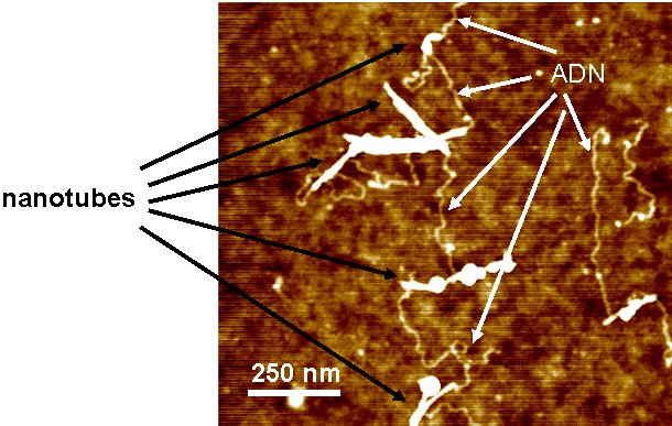
Atomic force microscopy image of DNA-carbon nanotube structures realized using streptavidin-biotin complexes.
![]() PHoCEA DRF 2024 - Tous droits réservés - Mentions légales - Ce site utilise Bootstrap
PHoCEA DRF 2024 - Tous droits réservés - Mentions légales - Ce site utilise Bootstrap
Dernière mise à jour : 26-04-2024
