Laboratoire Léon Brillouin
UMR12 CEA-CNRS, Bât. 563 CEA Saclay
91191 Gif sur Yvette Cedex, France
+33-169085241 llb-sec@cea.fr
Laboratoire Léon Brillouin
UMR12 CEA-CNRS, Bât. 563 CEA Saclay
91191 Gif sur Yvette Cedex, France
+33-169085241 llb-sec@cea.fr

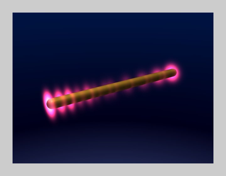
Optical field around a gold 40 nm in diameter and 4 microns in length nano rod, induced by an incident laser wave. (Équipe LEPO).
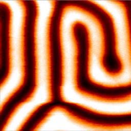
Future optics and electronics : Building a device (electronic, magnetic, photonic, sensor ...) at the atomic scale (nanometer) is the final step in miniaturization. In the laboratory nanofabrication techniques allow to carry out individual structures of a few atoms or molecules.
Beyond the reduction in size and the resulting increase in integration density, new properties appears at this scale, often of quantum origin, which can be used. Understanding the behavior of these "nano-objects", controlling their fabrication process or integration in devices and studying their properties are research topics carrying industrial issues for tomorrow.
The action of IRAMIS on the subject is facing a fundamental knowledge of the behavior of atomic or molecular systems and the search for new applications yet unimagined. An important activity of the IRAMIS concerns spin electronics (spintronics), with in particular the design and production of ultra-sensitive magnetic field sensors with multiple applications (non-destructive testing, security, speed sensors, sensors current ...).
Several IRAMIS teams are involved in calculations of the electronic structure (ab-initio , tight binding, Hückel methods, etc...) and more generally in the modeling of matter at the atomic scale, which also includes more phenomenological methods (empirical potentials, model Hamiltonians, etc...)
These modeling tools are mainly developed and used in physics (spectroscopy, transport, magnetism), chemistry (reactivity, dynamics) and for the study of materials (diffusion, growth, defects).
The "Theoretical spectroscopy" research group within LSI - Irradiated Solid Laboratory (Contact: Lucia Reining) is part of the heart of the ETSF structure (European Theoretical Spectroscopy Facility).
The topic "Electronic structure and atomistic modelisation" within the SPEC/GMT group (Contact: Cyrille Barreteau) gathers 4 research axis:
This research topic focuses on the development and study of:
Such studies use many techniques mastered within IRAMIS: thin film growth (in particular oxides), magnetic transport measurements, (polarized) neutron scattering, ... The characterization of magnetic sensors is performed in a "ultra low magnetic noise laboratory" necessary to the development of multiple applications: non-destructive testing, security, speed sensors, current sensors ....
The "Nanomagnetism and Oxides Laboratory" (LNO) within SPEC has its activity fully focused on this topic.
Multiferroic materials are multifunctional materials having simultaneously several "ferroic" properties: ferromagnetism, ferroelectricity and / or ferro-elasticity. Their development in thin layers allows to design functional devices, where their coupled properties can be used.
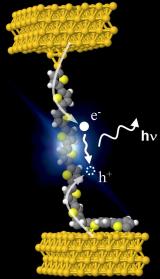
With organic and molecular electronics, a data processing based on various types of nano-objects (molecules, biomolecules, nanoparticles, carbon nanotubes, graphene,...) is emerging.
This means developing:
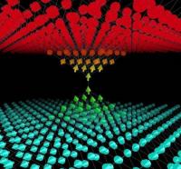
In the case illustrated here, one single molecule is connected to two electrodes spaced by 1 to 3 nm, the objectives are to master and understand the metal-molecule interface and the properties of the so positioned molecule. On this principle, single molecule LEDs have recently been studied: "Electroluminescence of a single polythiophene molecular wire suspended between the tip and the surface of a scanning tunneling microscope", © Guillaume Schull - IPCMS - CNRS / Université de Strasbourg.
![]() PHoCEA DRF 2024 - Tous droits réservés - Mentions légales - Ce site utilise Bootstrap
PHoCEA DRF 2024 - Tous droits réservés - Mentions légales - Ce site utilise Bootstrap
Dernière mise à jour : 07-04-2024